- 您现在的位置:买卖IC网 > Sheet目录1210 > DLP-HS-FPGA2 (DLP Design Inc)MODULE USB ADAPTER FOR FT2232H
�� �
�
�Memory�
�Write�
�Writes� 4�
�bytes� to� the�
�0�
�0x9n�
�Writes� 4� bytes� to� the� DDR2� SDRAM� starting� with� the�
�address� specified.� The� command� byte� is� OR’d� with� the�
�DDR�
�SDRAM�
�Most� Significant� Row� Address� bit� (24).�
�n� =� 0� the� Most� Sig� Row� Address� bit� is� low� (0x90)�
�n� =� 1� the� most� Sig� Row� Address� bit� is� high� (0x91)�
�1�
�2�
�3�
�4�
�5�
�6�
�7�
�0xah�
�0xam�
�0xal�
�0xd0�
�0xd1�
�0xd2�
�0xd3�
�Bits� 23-16� Middle� 8� bits� of� Row� Address� to� be� written� to�
�Bits� 15-12� Lower� 4� bits� of� Row� Address� to� be� written� to�
�Bits� 11-8� Upper� 4� bits� Column� Address� to� be� written� to�
�Bits� 7-2:� Lower� 6� bits� of� column� address� to� be� written� to�
�NOTE:� Refer� to� the� text� above� regarding� Column� Bits� 1�
�and� 0� (equates� to� 0xal� bits� 3-2).� Bits� 1-0:� Bank� Address�
�to� be� written� to�
�Data� Byte� 0� written� to� Address� Specified�
�Data� Byte� 1� written� to� Address� Specified� +� 1�
�Data� Byte� 2� written� to� Address� Specified� +� 2�
�Data� Byte� 3� written� to� Address� Specified� +� 3.� Returns�
�the� 4� bytes� written� followed� by� an� echo� back� of� the�
�command� and� address� data� sent.�
�NOTE:� If� the� memory� has� not� been� initialized,� the�
�command� returned� will� be� 0xE7� indicating� the� error.�
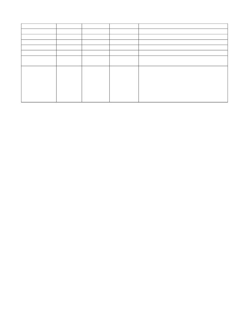
�The� USER� I/O� Pin� Read/Set/Clear� Commands� I/O� number� mapping� to� the� physical� I/O� pins� on� the�
�DLP-HS-FPGA� board� are� described� in� the� following� table:�
�TABLE� 2�
�User� I/O�
�I/O� Number�
�0x00� (0)�
�0x01� (1)�
�0x02� (2)�
�0x03� (3)�
�0x04� (4)�
�0x05� (5)�
�0x06� (6)�
�0x07� (7)�
�0x08� (8)�
�0x09� (9)�
�0x0A� (10)�
�0x0B� (11)�
�0x0C� (12)�
�0x0D� (13)�
�Rev.� 1.7� (May� 2011)�
�DLP-HS-�
�FPGA� Pin�
�J1� Pin� 2�
�J1� Pin� 3�
�J1� Pin� 4�
�J1� Pin� 5�
�J1� Pin� 6�
�J1� Pin� 7�
�J1� Pin� 8�
�J1� Pin� 9�
�J1� Pin� 10�
�J1� Pin� 12�
�J1� Pin� 13�
�J1� Pin� 14�
�J1� Pin� 15�
�J1� Pin� 16�
�XC3S200A�
�XC3S400A�
�Pin�
�D13�
�C13�
�D11�
�C12�
�C10�
�D9�
�C8�
�D8�
�A14�
�A13�
�A6�
�B6�
�C11�
�A11�
�XC3S200A�
�XC3S400A�
�Bank�
�0�
�0�
�0�
�0�
�0�
�0�
�0�
�0�
�0�
�0�
�0�
�0�
�0�
�0�
�12�
�FPGA� Pin� Configurations� Available�
�Digital� Input,� Output,� Differential� Pair� 0+�
�Digital� Input,� Output,� Differential� Pair� 0-�
�Digital� Input,� Output,� Differential� Pair� 1-�
�Digital� Input,� Output,� Differential� Pair� 1+�
�Digital� Input,� Output,� Differential� Pair� 2+,�
�Global� Clock�
�Digital� Input,� Output,� Differential� Pair� 2-,�
�Global� Clock�
�Digital� Input,� Output,� Differential� Pair� 3+,�
�Global� Clock�
�Digital� Input,� Output,� Differential� Pair� 3-,�
�Global� Clock�
�Digital� Input,� Output,� Differential� Pair� 4+�
�Digital� Input,� Output,� Differential� Pair� 4-�
�Digital� Input,� Output,� Differential� Pair� 5+�
�Digital� Input,� Output,� Differential� Pair� 5-�
�Digital� Input,� Output,� Differential� Pair� 6+�
�Digital� Input,� Output,� Differential� Pair� 6-�
�?� DLP� Design,� Inc.�
�发布紧急采购,3分钟左右您将得到回复。
相关PDF资料
DLP-IOR4
MODULE LATCHING-RELAY 4-CH
DLP-TEMP-G
MODULE DATA-ACQUISITION 3-CH
DLP-TXRX-G
MODULE USB-TO-TTL SRL UART CONV
DLP-USB1232H
MODULE USB-TO-UART/FIFO HS 18DIP
DLP-USB232M-G
MODULE USB-TO-TTL SRL UART CONV
DLP-USB232R
MODULE USB-TO-SRL UART 18-DIP
DLP-USB245M-G
MODULE USB-TO-TTL PARL FIFO CONV
DLP-USB245R
MODULE USB-TO-PARL FIFO 18-DIP
相关代理商/技术参数
DLP-HS-FPGA3
功能描述:可编程逻辑 IC 开发工具 USB-to-FPGA Development Module
RoHS:否 制造商:Altera Corporation 产品:Development Kits 类型:FPGA 工具用于评估:5CEFA7F3 接口类型: 工作电源电压:
DLP-HS-FPGA-A
功能描述:FPGA Embedded Module Spartan-3A, XC3S200A FT2232H 66MHz 32MB 制造商:dlp design inc. 系列:FPGA 零件状态:有效 模块/板类型:FPGA,USB ?? 核心处理器:Spartan-3A,XC3S200A 协处理器:FT2232H 速度:66MHz 闪存大小:- RAM 容量:32Mb 连接器类型:USB - B,引脚接头 大小/尺寸:3" x 1.2"(76.2mm x 30.5mm) 工作温度:0°C ~ 70°C 标准包装:1
DLP-IO14
功能描述:数据记录与采集 14-Channel Data-Acq Module
RoHS:否 制造商:Lantronix 描述/功能:Analog device server 显示器类型:None 电流额定值:
DLP-IO16
功能描述:界面模块 USB/Micro Dev Board
RoHS:否 制造商:4D Systems 产品:Serial Converters 通道/端口数量: 数据速率: 接口类型:USB, UART 工作电源电压:3.3 V, 5 V 最大工作温度:
DLP-IO20
功能描述:数据记录与采集 USB-BASED 20-CHANNEL DATA ACQUISITION MOD RoHS:否 制造商:Lantronix 描述/功能:Analog device server 显示器类型:None 电流额定值:
DLP-IO26
功能描述:开发板和工具包 - PIC / DSPIC USB/Micro Dev Board
RoHS:否 制造商:Microchip Technology 产品:Starter Kits 工具用于评估:chipKIT 核心:Uno32 接口类型: 工作电源电压:
DLP-IO8
功能描述:界面模块 USB-BASED 8-CHANL DATA ACQUSITION MODL
RoHS:否 制造商:4D Systems 产品:Serial Converters 通道/端口数量: 数据速率: 接口类型:USB, UART 工作电源电压:3.3 V, 5 V 最大工作温度:
DLP-IO8-G
功能描述:数据记录与采集 USB-BASED 8-CHANL DATA ACQUSITION MODL RoHS:否 制造商:Lantronix 描述/功能:Analog device server 显示器类型:None 电流额定值: